Solving Real World's Problems Through Advance Nanomaterials
Welcome to the Jun Li Research Group Homepage
Research in our laboratory is in the interdisciplinary field of nanoscience and nanotechnology, with an emphasis on the development of micro-/nano- devices for analytical, biomedical, electronic, and energy conversion/storage applications. Our research covers (1) nanomaterials growth, (2) device fabrication and characterization, and (3) applications development. These projects are in close collaboration with academia, industry, and government labs.
Nanomaterials Growth
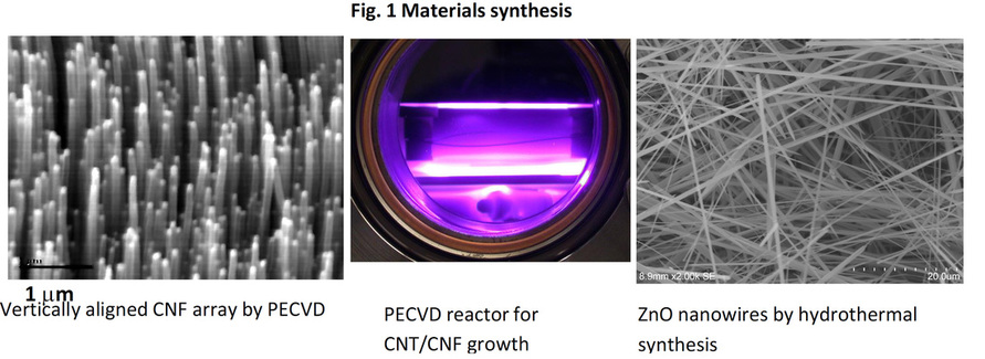
Our nanomaterials synthesis work is focused on preparing high-aspect ratio nanowires (NWs). A major effort is on exploring new methods to grow nanowires deterministically on solid substrates with controlled diameter, length, and orientation (particularly in free-standing vertical orientation) for device applications. The nanowire materials include carbon nanotubes (CNTs), carbon nanofibers (CNFs), semiconducting inorganic crystalline nanowires (s-NWs), and metallic nanowires (m-NWs). The methods include thermal chemical vapor deposition (CVD), plasma enhanced chemical vapor deposition (PECVD), and electrochemical deposition. Another effort is on large-quantity synthesis of NWs with hydrothermal method. NW materials such as ZnO, Bi2Te3, MnO2, etc. have been prepared for various applications.
Research in our laboratory is in the interdisciplinary field of nanoscience and nanotechnology, with an emphasis on the development of micro-/nano- devices for analytical, biomedical, electronic, and energy conversion/storage applications. Our research covers (1) nanomaterials growth, (2) device fabrication and characterization, and (3) applications development. These projects are in close collaboration with academia, industry, and government labs.
Nanomaterials Growth
Our nanomaterials synthesis work is focused on preparing high-aspect ratio nanowires (NWs). A major effort is on exploring new methods to grow nanowires deterministically on solid substrates with controlled diameter, length, and orientation (particularly in free-standing vertical orientation) for device applications. The nanowire materials include carbon nanotubes (CNTs), carbon nanofibers (CNFs), semiconducting inorganic crystalline nanowires (s-NWs), and metallic nanowires (m-NWs). The methods include thermal chemical vapor deposition (CVD), plasma enhanced chemical vapor deposition (PECVD), and electrochemical deposition. Another effort is on large-quantity synthesis of NWs with hydrothermal method. NW materials such as ZnO, Bi2Te3, MnO2, etc. have been prepared for various applications.
Device Fabrication and Characterization
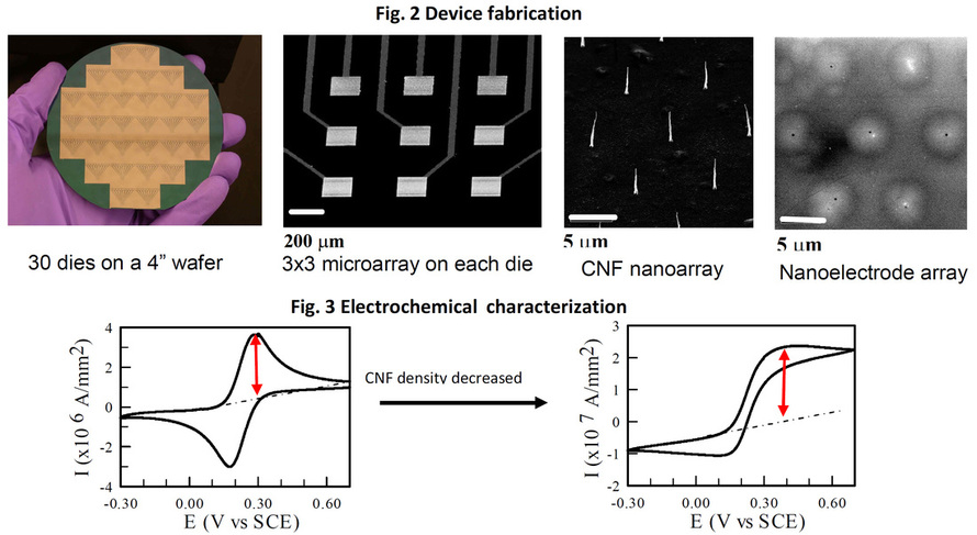
We employ conventional solid-state micro-/nano- fabrication techniques including lithography, CVD/PVD, plasma and wet chemical etching, sputtering, and chemical mechanical polishing. In addition, nonconventional methods such as soft-lithography, imprinting, templating, electrochemical etching/deposition, and chemical functionalization are investigated. Most fabrication processes employ a bottom-up method using massive arrays of vertically aligned CNTs and NWs on patterned substrates. The electronic, physical, and chemical properties and device performance are studied with electrochemistry, I-V measurements, optical spectroscopy, electron microscopy, and scanning probe microscopy. For biomaterials and biomedical devices, experiments involving molecular biochemistry, cell/tissue culture, and in-vivo animal experiments are carried in our lab or through collaborations.
We employ conventional solid-state micro-/nano- fabrication techniques including lithography, CVD/PVD, plasma and wet chemical etching, sputtering, and chemical mechanical polishing. In addition, nonconventional methods such as soft-lithography, imprinting, templating, electrochemical etching/deposition, and chemical functionalization are investigated. Most fabrication processes employ a bottom-up method using massive arrays of vertically aligned CNTs and NWs on patterned substrates. The electronic, physical, and chemical properties and device performance are studied with electrochemistry, I-V measurements, optical spectroscopy, electron microscopy, and scanning probe microscopy. For biomaterials and biomedical devices, experiments involving molecular biochemistry, cell/tissue culture, and in-vivo animal experiments are carried in our lab or through collaborations.
Add Title Here
Add Text Here
Add Text Here
